- 您现在的位置:买卖IC网 > Sheet目录1196 > AT73C224-EK1 (Atmel)KIT EVALUATION FOR AT73C224
�� �
�
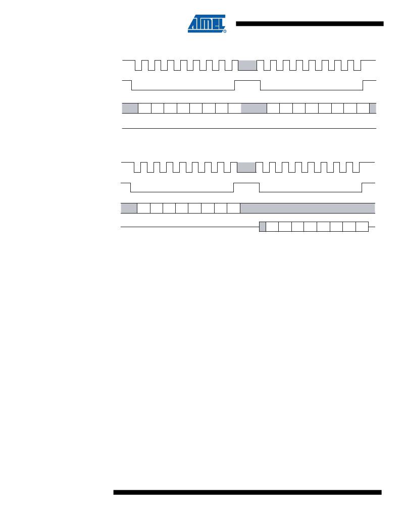
�Figure� 5-7.�
�SCK�
�SCS�
�SPI� Read� and� Write� Operations�
�SDI�
�0�
�A6�
�A5�
�A4�
�A3�
�A2�
�A1�
�A0�
�D7�
�D6�
�D5�
�D4�
�D3�
�D2�
�D1�
�D0�
�SDO�
�Hz�
�SPI� Write�
�SCK�
�SCS�
�SDI�
�1�
�A6�
�A5�
�A4�
�A3�
�A2�
�A1�
�A0�
�Hz�
�SDO�
�D7�
�D6�
�D5�
�D4�
�D3�
�D2�
�D1�
�D0�
�SPI� Read�
�The� first� byte� of� a� pair� is� the� command/address� byte.� The� most� significant� bit� of� this� byte� indi-�
�cates� register� read� when� 1� and� register� write� when� 0.� The� remaining� seven� bits� of� the�
�command/address� byte� indicate� the� address� of� the� register� to� be� accessed.�
�The� second� byte� of� the� pair� is� the� data� byte.� During� a� read� operation,� the� SDO� becomes� active�
�and� the� 8-bit� contents� of� the� register� are� driven� out� MSB� first.� The� SDO� will� be� in� high� imped-�
�ance� on� either� the� falling� edge� of� SCK� following� the� LSB� or� the� rising� edge� of� SCS,� whichever�
�occurs� first.�
�SDI� is� a� don't� care� during� the� data� portion� of� read� operations.� During� write� operations,� data� is�
�driven� into� the� AT73C224-x� via� the� SDI� pin,� MSB� first.� The� SDO� pin� will� remain� in� high� imped-�
�ance� during� write� operations.� Data� always� transitions� with� the� falling� edge� of� the� clock� and� is�
�latched� on� the� rising� edge.� The� clock� should� return� to� a� logic� high� when� no� transfer� is� in�
�progress.�
�?� Continuous� clocking� :� In� normal� operation,� the� SCK� should� not� transition� out� of� byte� transfer�
�periods.� However,� in� test� mode,� the� SCK� is� used� as� the� main� clock.� This� implies� that� all� data�
�transfers� must� be� controlled� by� the� assertion� of� the� SCS� pin.�
�?� 3-wire� operation� :� SDI� and� SDO� can� be� treated� as� two� separate� lines� or� wired� together� if� the�
�master� is� capable� of� tri-stating� its� output� during� the� data-byte� transfer� of� a� read� operation.�
�?� SCK� vs� internal� clock� rates� :� It� is� very� likely� that� the� bit� rate� commanded� by� SCK� will� be�
�much� higher� than� the� internal� clock� (900� kHz/64)� used� to� read� and� write� the� registers.� This�
�implies� that� a� minimal� delay� between� byte� transfers� must� be� imposed� to� allow� some� time� to�
�decode� the� address� and� actually� access� the� physical� register.� It� is� not� acceptable� to� sample�
�SCK� with� the� internal� clock.�
�16�
�AT73C224�
�6266A–PMAAC–08-Sep-08�
�发布紧急采购,3分钟左右您将得到回复。
相关PDF资料
AT73C239-EK
KIT EVAL FOR AT73C239
AT73C240-EK1
KIT EVALUATION FOR AT73C240
AT73C246-EK1
KIT EVALUATION FOR AT73C246
AT85DVK-07
KIT DEV FOR AT85C51SND3
AT85RFD-07
REFERENCE DESIGN FOR AT85C51SND3
AT88CK101BK8
BOARD KIT CRYPTO W/SOIC SKT
AT88CK101STK8
BOARD KIT CRYPTO W/SOIC&MICRO
AT88CK109BK8
BOARD KIT CRYPTO W/2 SOIC SKTS
相关代理商/技术参数
AT73C224-F
制造商:ATMEL 制造商全称:ATMEL Corporation 功能描述:Power Management and Analog Companions (PMAAC)
AT73C224-G
制造商:ATMEL 制造商全称:ATMEL Corporation 功能描述:Power Management and Analog Companions (PMAAC)
AT73C224-H
制造商:ATMEL 制造商全称:ATMEL Corporation 功能描述:Power Management and Analog Companions (PMAAC)
AT73C225J
功能描述:电池管理 Monolithic numeric RoHS:否 制造商:Texas Instruments 电池类型:Li-Ion 输出电压:5 V 输出电流:4.5 A 工作电源电压:3.9 V to 17 V 最大工作温度:+ 85 C 最小工作温度:- 40 C 封装 / 箱体:VQFN-24 封装:Reel
AT73C237
功能描述:其他电源管理 NGD : MONOLITHIC NUMERIC IC RoHS:否 制造商:Texas Instruments 输出电压范围: 输出电流:4 mA 输入电压范围:3 V to 3.6 V 输入电流: 功率耗散: 工作温度范围:- 40 C to + 110 C 安装风格:SMD/SMT 封装 / 箱体:VQFN-48 封装:Reel
AT73C238
功能描述:电池管理 Monolithic numeric RoHS:否 制造商:Texas Instruments 电池类型:Li-Ion 输出电压:5 V 输出电流:4.5 A 工作电源电压:3.9 V to 17 V 最大工作温度:+ 85 C 最小工作温度:- 40 C 封装 / 箱体:VQFN-24 封装:Reel
AT73C239
功能描述:其他电源管理 NGD MONOLITHIC NUMERIC IC RoHS:否 制造商:Texas Instruments 输出电压范围: 输出电流:4 mA 输入电压范围:3 V to 3.6 V 输入电流: 功率耗散: 工作温度范围:- 40 C to + 110 C 安装风格:SMD/SMT 封装 / 箱体:VQFN-48 封装:Reel
AT73C239_07
制造商:ATMEL 制造商全称:ATMEL Corporation 功能描述:Power Management and Analog Companions (PMAAC)